The Most Insane Machine on Earth: Inside ASML’s EUV Lithography Systems
Before we dive into ASML’s EUV machines, it helps to understand how the modern semiconductor ecosystem is structured. Consider a different example: Apple designs its SoCs (System-on-Chip), TSMC (Taiwan Semiconductor Manufacturing Company) manufactures them, and ASML provides the EUV lithography equipment needed for advanced nodes.
The same dynamic holds for Nvidia and AI GPUs. Nvidia’s Blackwell GPUs require TSMC’s 5 nm or smaller process technology. TSMC, in turn, relies on ASML’s EUV tools to print the dense transistor layouts. A delay or shortage at any point would slow the entire industry.
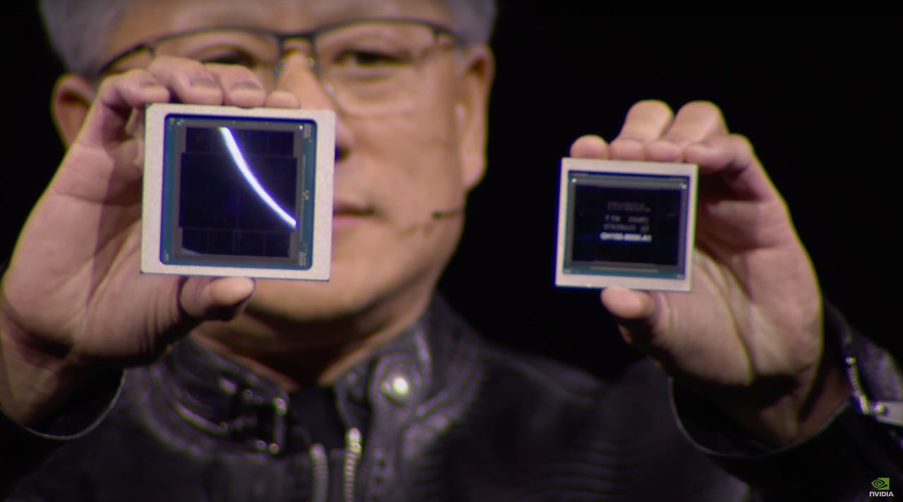
Nvidia co-founder and CEO Jensen Huang compares the new Blackwell GPU to its predecessor, H100 "Hopper," at GTC 2024.
What Exactly Is an ASML EUV Machine?
In the world of semiconductor manufacturing, nothing else even comes close to the engineering scale and complexity of ASML’s extreme ultraviolet (EUV) lithography machines. These behemoths are the core tools that print the world’s most advanced computer chips: from the processors in your smartphone to the AI accelerators that train large language models.


At its core, an EUV lithography system is the machine that “prints” circuit patterns on silicon wafers using extreme ultraviolet light (EUV, ~13.5 nm wavelength). This short wavelength lets manufacturers create features that are only a few nanometers wide, essential for modern chips below ~7 nm node. (Wikipedia)
Instead of traditional lenses, these tools use ultra‑precise mirrors to project patterns: each must be polished so perfectly that even if scaled up to the size of a country, the largest imperfection would be smaller than a millimeter. (ASML)
This precision is not optional, it’s the only way to achieve the accuracy needed to fabricate billions of transistors in areas smaller than a dust mite.
EUV lithography requires a unique combination of extreme ultraviolet light generation, atomic-scale mirrors, vacuum operation, and nanometer-precision mechanics that only ASML has successfully developed, integrated, and industrialized at scale.
The Insane Scale: Physically and Economically
Size & Logistics
- Weight: ~180+ metric tons (as heavy as a couple of full‑size cars stacked). (Medium)
- Dimensions: Roughly the size of a bus, often ~10 m long and several meters high and wide. (Gadget Help)
- Transport: Machines ship in dozens of freight containers and can require multiple cargo planes, trucks, and months of on‑site assembly at customer fabs. (Medium)
- Components: ~100,000 parts, >3,000 cables, ~40,000 bolts, and ~2 km of hosing. (Medium)
Cost: It’s Not a Typo
These are among the most expensive machines ever created:
| System Type | Typical Cost (USD) | Purpose |
|---|---|---|
| EUV (standard) | ~$180M-$250M | Advanced chips ~7nm-3nm nodes. (FourWeekMBA) |
| High‑NA EUV | ~$350M-$400M | Next‑gen resolution toward ~2nm/1.4nm. (FourWeekMBA) |
| DUV systems | ~$5M-$90M | Older litho used for mature nodes (auto, IoT). (FourWeekMBA) |
Yes, prices routinely dwarf the cost of passenger aircraft and rival advanced scientific infrastructure. (www.whatjobs.com)
How It Actually Works (Without Exaggeration)
Many online videos dramatize the process, but here’s the real engineering summary:
- Tin droplet generation: Microscopic droplets of molten tin are fired into a vacuum. (artificialintelligencenews.in)
- Laser conversion: High‑power CO₂ lasers hit the droplets, creating a plasma hotter than the Sun’s surface that emits EUV light. (artificialintelligencenews.in)
- Optics system: EUV light reflects off precision mirrors and is projected through a mask that has the chip’s pattern. (Wikipedia)
- Wafer exposure: The pattern transfers onto a light‑sensitive photoresist on the silicon wafer. (GadgetMates)
- Layer by layer: This happens hundreds to thousands of times per wafer, stacking complex circuits. (GadgetMates)
From an engineering perspective, EUV lithography is one of the most complex light‑based manufacturing processes ever devised. It requires vacuum optics, nanometer‑precision stages, and lasers synchronized at tens of thousands of pulses per second. (artificialintelligencenews.in)
This is how the world’s most advanced chips are made.
ASML’s High-NA EUV TWINSCAN EXE uses extreme ultraviolet light, ultra-precise optics, and massive engineering to print features at 8 nm resolution, boosting imaging contrast by ~40% over previous EUV systems. Bigger machine, smaller transistors and the foundation for the next generation of CPUs, GPUs, and AI chips.
What This Means for Technology
These machines aren’t just expensive curiosities, they are the foundations of modern computing:
- Every advanced chip in your smartphones, laptops, AI accelerators, and supercomputers relies on patterns printed by EUV lithography. (www.whatjobs.com)
- Major fabs (TSMC, Samsung, Intel) buy only ASML’s EUV tools because no one else offers the same resolution or throughput. (golden.com)
- High‑NA machines are now entering production, pushing the industry toward sub‑2 nm nodes. (FourWeekMBA)
This has global strategic value: access to these machines literally determines which countries and companies can build the most advanced semiconductors. (The Guardian)
Why It Took Decades and Billions
Developing EUV lithography wasn’t just a company project, it was more than 30 years of R&D across hundreds of suppliers world‑wide. ASML integrates optics from ZEISS, lasers from specialized vendors, vibration isolation systems, and clean‑room assembly that borders on laboratory‑precision machining. (ASML)
The result is a supply chain and engineering ecosystem so specialized that replicating it would take enormous time and capital.
Bottom Line: The Most Crucial Machine You’ve Never Seen
ASML’s EUV lithography systems are not sci‑fi tech, they are industrial reality:
- They enable the chips powering AI, phones, and cloud computing. (www.whatjobs.com)
- They cost hundreds of millions and take months to install. (FourWeekMBA)
- They represent decades of global engineering collaboration. (ASML)
Next time you think about a smartphone or neural net, remember: the invisible giant behind the scenes is this room‑sized lithography machine, built with the highest engineering precision humanity has ever managed.
References & Further Reading
🔗 ASML technology overview: optics, numerical aperture, and lithography principles (ASML) Lenses & Mirrors in EUV Lithography
🔗 Pricing breakdown: DUV vs. EUV vs. High‑NA ASML Machine Pricing Explained
🔗 EUV basics: how extreme ultraviolet lithography works Extreme Ultraviolet Lithography Explained
🔗 Industry impact: ASML’s machines and global chipmaking The EUV Machine That Built the AI Revolution
If you found this useful, please cite this as:
Rossetti, Simone (Jan 2026). The Most Insane Machine on Earth: Inside ASML’s EUV Lithography Systems. https://rossettisimone.github.io.
or as a BibTeX entry:
@article{rossetti2026the-most-insane-machine-on-earth-inside-asml-s-euv-lithography-systems,
  title   = {The Most Insane Machine on Earth: Inside ASML’s EUV Lithography Systems},
  author  = {Rossetti, Simone},
  year    = {2026},
  month   = {Jan},
  url     = {https://rossettisimone.github.io/blog/2026/the-most-insane-machine/}
}
Enjoy Reading This Article?
Here are some more articles you might like to read next:
Subscribe to be notified of future articles: